6-Layer Copper Coin Embedded PCB 1.0mm – M6 & IT180 Hybrid with ENIG Finish for 5G and Automotive
1. Introduction
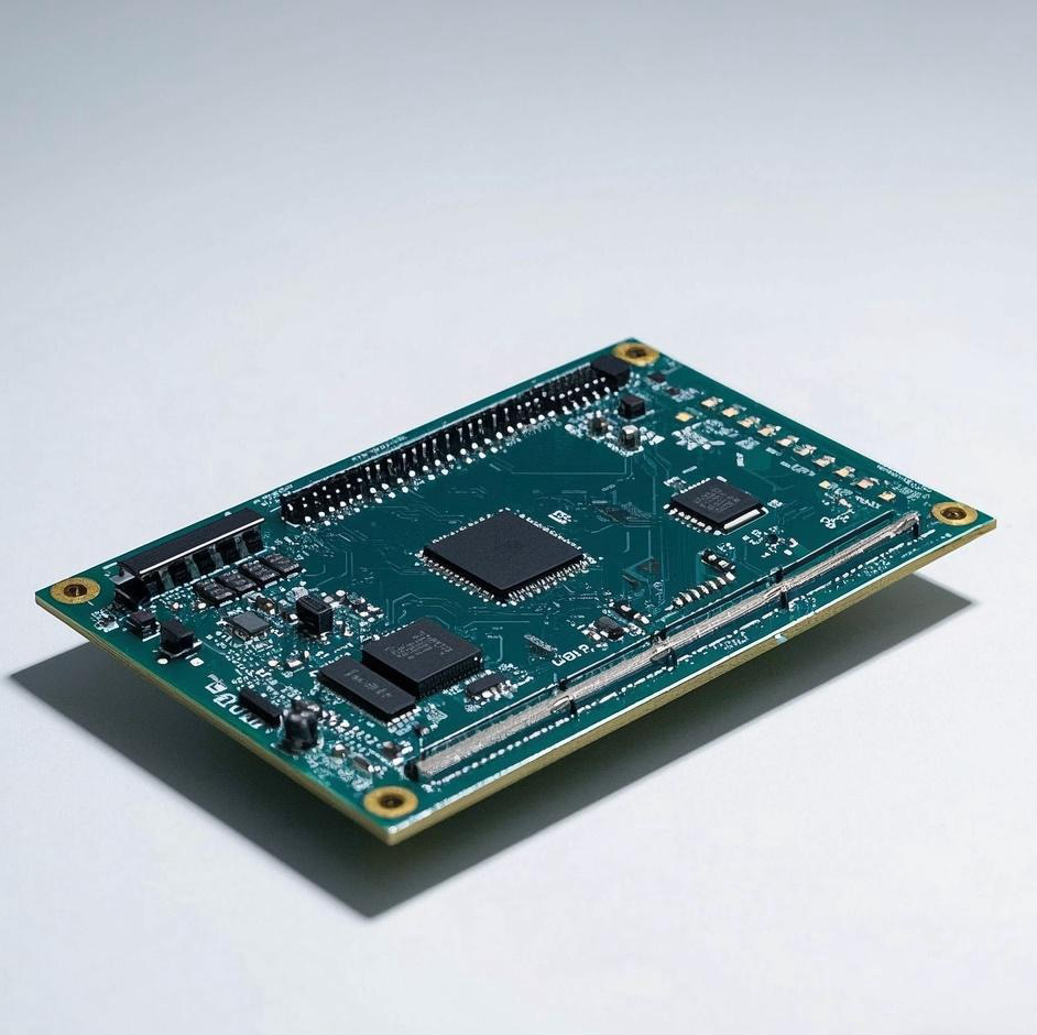
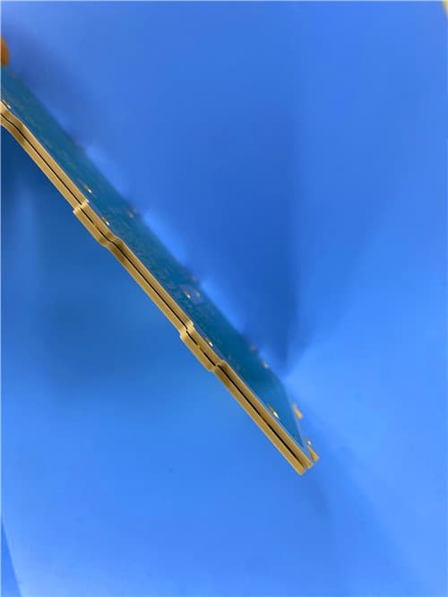
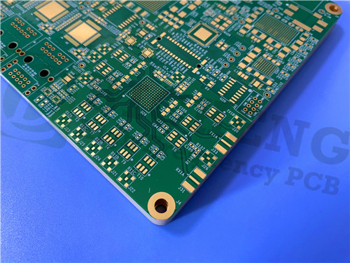
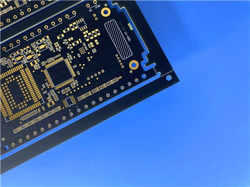
This advanced printed circuit board utilizes a hybrid material structure combining M6 high-speed material and high-Tg FR-4 (IT-180), creating a 6-layer construction with exceptional electrical and thermal performance. The board incorporates an embedded copper coin in the center for enhanced thermal management, along with resin-filled and capped vias for improved reliability and surface planarity. This design supports complex circuit requirements while maintaining compatibility with standard FR-4 processing technology.
2. Key Features
Hybrid material stackup: M6 (Dk 3.61) and IT-180 (Dk 4.17) cores
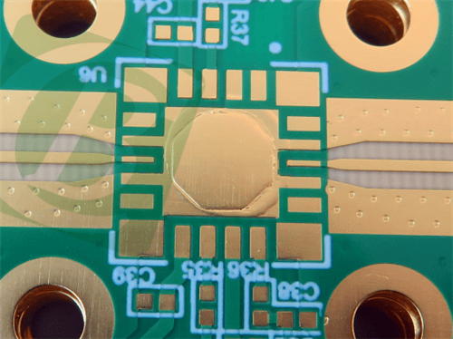
Embedded copper coin for superior thermal dissipation
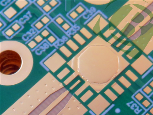
All vias resin-filled and capped
Mixed copper weights: 1oz outer layers, 0.5oz/1oz inner layers
High Tg value >185°C (DSC method)
Thermal decomposition temperature: 410°C
UL 94V-0 flammability rating
Halogen-free and RoHS compliant
3. Benefits
Excellent thermal management for high-power applications
Stable dielectric constant across frequency range
Compatible with traditional FR-4 processing technology
Supports complex multilayer designs (4-30 layers)
Reliable performance in harsh environments
Green manufacturing compliance
Compatible with resistive foils
4. PCB Construction Details
| Parameter | Specification |
| Base Material | M6 High Speed Material + High Tg FR-4 |
| Layer Count | 6 Layers |
| Board Dimensions | 100mm × 50mm (±0.15mm) |
| Min. Trace/Space | 4 mil / 5 mil |
| Min. Hole Size | 0.3 mm |
| Blind Vias | No |
| Finished Board Thickness | 1.0 mm |
| Finished Cu Weight | Inner Layers: 1oz/0.5oz mixed, Outer Layers: 1oz |
| Via Plating Thickness | 20 μm |
| Surface Finish | ENIG (Electroless Nickel Immersion Gold) |
| Top/Bottom Silkscreen | White |
| Top/Bottom Solder Mask | Green |
| Special Feature 1 | Copper coin embedded in the center of PCB |
| Special Feature 2 | All vias are resin filled and capped |
| Electrical Test | 100% tested prior to shipment |
5. PCB Stackup (6-Layer Rigid Structure)
| Layer | Material Type | Thickness | Dielectric Constant | Copper Thickness |
| Top Layer | Copper Foil | - | - | 35 μm |
| - | R5775G (M6) Core | 0.25 mm | 3.61 | - |
| Inner Layer 1 | Copper | - | - | 18 μm |
| - | Prepreg (1080, 64%) × 2 | 0.14 mm | 3.72 | - |
| Inner Layer 2 | Copper | - | - | 35 μm |
| - | IT-180 Core | 0.1 mm | 4.17 | - |
| Inner Layer 3 | Copper | - | - | 35 μm |
| - | Prepreg (1080, 64%) × 2 | 0.14 mm | 3.72 | - |
| Inner Layer 4 | Copper | - | - | 18 μm |
| - | IT-180 Core | 0.1 mm | 4.17 | - |
| Bottom Layer | Copper Foil | - | - | 35 μm |
6. PCB Statistics:
Components: 75
Total Pads: 224
Thru Hole Pads: 172
Top SMT Pads: 52
Bottom SMT Pads: 36
Vias: 72
Nets: 15
7. Typical Applications
5G communication base stations (millimeter-wave antennas, RF front-ends)
Automotive electronics (77GHz millimeter-wave radar, ADAS)
Networking & communications equipment
Aerospace & defense systems
8. Quality Assurance
Artwork Format: Gerber RS-274-X
Accepted Standard: IPC-Class-2
Availability: Worldwide
|
.jpg)
.jpg)